- 您现在的位置:买卖IC网 > Sheet目录3818 > PIC18F4620-I/ML (Microchip Technology)IC MCU FLASH 32KX16 44QFN
1996 Microchip Technology Inc.
DS30412C-page 185
PIC17C4X
Applicable Devices 42 R42 42A 43 R43 44
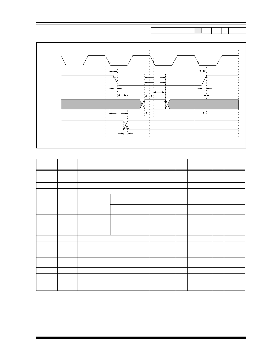
FIGURE 19-3: CLKOUT AND I/O TIMING
TABLE 19-3:
CLKOUT AND I/O TIMING REQUIREMENTS
Parameter
No.
Sym
Characteristic
Min
Typ
Max
Units Conditions
10
TosH2ckL
OSC1
↓ to CLKOUT↓
—
15
30
ns
Note 1
11
TosH2ckH
OSC1
↓ to CLKOUT↑
—
15
30
ns
Note 1
12
TckR
CLKOUT rise time
—
5
15
ns
Note 1
13
TckF
CLKOUT fall time
—
5
15
ns
Note 1
14
TckH2ioV
CLKOUT
↑ to Port
out valid
PIC17CR42/42A/43/
R43/44
—
0.5TCY + 20
ns
Note 1
PIC17LCR42/42A/43/
R43/44
—
0.5TCY + 50
ns
Note 1
15
TioV2ckH
Port in valid before
CLKOUT
↑
PIC17CR42/42A/43/
R43/44
0.25TCY + 25
—
ns
Note 1
PIC17LCR42/42A/43/
R43/44
0.25TCY + 50
—
ns
Note 1
16
TckH2ioI
Port in hold after CLKOUT
↑
0
—
ns
Note 1
17
TosH2ioV
OSC1
↓ (Q1 cycle) to Port out valid
—
100
ns
18
TosH2ioI
OSC1
↓ (Q2 cycle) to Port input invalid
(I/O in hold time)
0
—
ns
19
TioV2osH
Port input valid to OSC1
↓
(I/O in setup time)
30
—
ns
20
TioR
Port output rise time
—
10
35
ns
21
TioF
Port output fall time
—
10
35
ns
22
TinHL
INT pin high or low time
25 *
—
ns
23
TrbHL
RB7:RB0 change INT high or low time
25 *
—
ns
*
These parameters are characterized but not tested.
Data in “Typ” column is at 5V, 25
°C unless otherwise stated. These parameters are for design guidance only and are not
tested.
These parameters are for design guidance only and are not tested, nor characterized.
Note 1:
Measurements are taken in EC Mode where CLKOUT output is 4 x TOSC.
OSC1
OSC2
I/O Pin
(input)
I/O Pin
(output)
Q4
Q1
Q2
Q3
10
13
14
17
20, 21
22
23
19
18
15
11
12
16
old value
new value
In EC and RC modes only.
发布紧急采购,3分钟左右您将得到回复。
相关PDF资料
PIC24HJ256GP210-I/PT
IC PIC MCU FLASH 128KX16 100TQFP
PIC24HJ128GP310A-I/PF
IC PIC MCU FLASH 128KB 100-TQFP
DSPIC33FJ128GP310-I/PF
IC DSPIC MCU/DSP 128K 100TQFP
PIC16C66-20I/SO
IC MCU OTP 8KX14 PWM 28SOIC
DSPIC33FJ128MC510-I/PT
IC DSPIC MCU/DSP 128K 100TQFP
PIC16C66-20I/SP
IC MCU OTP 8KX14 PWM 28DIP
PIC18LF2620-I/SP
IC MCU FLASH 32KX16 28SDIP
PIC16F877-04I/P
IC MCU FLASH 8KX14 EE 40DIP
相关代理商/技术参数
PIC18F4620-I/P
功能描述:8位微控制器 -MCU 64KB 3968 RAM 36 I/O RoHS:否 制造商:Silicon Labs 核心:8051 处理器系列:C8051F39x 数据总线宽度:8 bit 最大时钟频率:50 MHz 程序存储器大小:16 KB 数据 RAM 大小:1 KB 片上 ADC:Yes 工作电源电压:1.8 V to 3.6 V 工作温度范围:- 40 C to + 105 C 封装 / 箱体:QFN-20 安装风格:SMD/SMT
PIC18F4620-I/P
制造商:Microchip Technology Inc 功能描述:IC 8BIT FLASH MCU 18F4620 DIP40
PIC18F4620-I/PT
功能描述:8位微控制器 -MCU 64KB 3968 RAM 36 I/O RoHS:否 制造商:Silicon Labs 核心:8051 处理器系列:C8051F39x 数据总线宽度:8 bit 最大时钟频率:50 MHz 程序存储器大小:16 KB 数据 RAM 大小:1 KB 片上 ADC:Yes 工作电源电压:1.8 V to 3.6 V 工作温度范围:- 40 C to + 105 C 封装 / 箱体:QFN-20 安装风格:SMD/SMT
PIC18F4620-I/PT
制造商:Microchip Technology Inc 功能描述:IC 8BIT FLASH MCU 18F4620 TQFP44
PIC18F4620T-I/ML
功能描述:8位微控制器 -MCU 64KB 3968 RAM 36 I/O RoHS:否 制造商:Silicon Labs 核心:8051 处理器系列:C8051F39x 数据总线宽度:8 bit 最大时钟频率:50 MHz 程序存储器大小:16 KB 数据 RAM 大小:1 KB 片上 ADC:Yes 工作电源电压:1.8 V to 3.6 V 工作温度范围:- 40 C to + 105 C 封装 / 箱体:QFN-20 安装风格:SMD/SMT
PIC18F4620T-I/PT
功能描述:8位微控制器 -MCU 64KB 3968 RAM 36 I/O RoHS:否 制造商:Silicon Labs 核心:8051 处理器系列:C8051F39x 数据总线宽度:8 bit 最大时钟频率:50 MHz 程序存储器大小:16 KB 数据 RAM 大小:1 KB 片上 ADC:Yes 工作电源电压:1.8 V to 3.6 V 工作温度范围:- 40 C to + 105 C 封装 / 箱体:QFN-20 安装风格:SMD/SMT
PIC18F4680-E/ML
功能描述:8位微控制器 -MCU 64KB 3328 RAM w/ECAN RoHS:否 制造商:Silicon Labs 核心:8051 处理器系列:C8051F39x 数据总线宽度:8 bit 最大时钟频率:50 MHz 程序存储器大小:16 KB 数据 RAM 大小:1 KB 片上 ADC:Yes 工作电源电压:1.8 V to 3.6 V 工作温度范围:- 40 C to + 105 C 封装 / 箱体:QFN-20 安装风格:SMD/SMT
PIC18F4680-E/P
功能描述:8位微控制器 -MCU 64KB 3328 RAM w/ECAN RoHS:否 制造商:Silicon Labs 核心:8051 处理器系列:C8051F39x 数据总线宽度:8 bit 最大时钟频率:50 MHz 程序存储器大小:16 KB 数据 RAM 大小:1 KB 片上 ADC:Yes 工作电源电压:1.8 V to 3.6 V 工作温度范围:- 40 C to + 105 C 封装 / 箱体:QFN-20 安装风格:SMD/SMT